


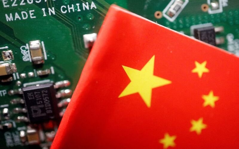
U.S. finalizes rules to prevent China from benefiting from $52 billion in chip funding. On Friday, the United States Department of Commerce will publish its final guidelines to ban China and other nations regarded as a threat to American national security from using subsidies offered to the semiconductor manufacturing industry.
Before the Biden administration can begin doling out $39 billion in subsidies for semiconductor production, the government must first clear the last hurdle: the regulation. The historic “Chips and Science” law allots $52.7 billion for the production of semiconductors in the United States, as well as for research and development of the workforce.
The regulation, first proposed in March, establishes “guardrails” by preventing recipients of U.S. funding from investing in the expansion of semiconductor manufacturing in countries like China and Russia that are of concern to the United States. It also prevents recipients of incentive funds from engaging in joint research or technology licensing efforts with foreign entities that concern the United States.
In October 2022, the department imposed additional export regulations to slow down Beijing’s technological and military advancements by cutting off China’s access to specific semiconductor chips manufactured using equipment from the United States.
The Secretary of Commerce Gina Raimondo delivered the following statement to Congress on Tuesday: “We need to be absolutely vigilant that not a penny of this helps China to get ahead of us.”
The Commerce Department has the authority to take back government prizes if the recipients of those awards breach restrictions.
Raimondo stated that she is doing everything possible to get the prizes accepted as quickly as possible.
“I feel the pressure,” said Raimondo. “I feel the pressure.” Although we are running behind schedule, we must get it right. And even if it takes us another month or a few extra weeks to get it right, I will defend that decision because I believe it is essential.
For ten years, the legislation forbids funding recipients from considerably increasing their semiconductor manufacturing capacity in countries outside of the European Union that are of concern. Additionally, it prevents beneficiaries from engaging in collaborative research or technology licensing endeavors with foreign companies. On the other hand, it does not prohibit recipients from utilizing international standards, patent licensing, foundry services, or packaging services.
According to the final guidelines, expanding material semiconductor manufacturing capacity in leading-edge and sophisticated facilities in foreign nations of concern is prohibited for ten years. It also makes it clear that the creation of wafers is included in the manufacturing of semiconductors.
The final rule requires an increased capacity for the fabrication of semiconductors by constructing a cleanroom or some other type of physical space. Material expansions are defined as an increase of more than 5% production capacity.
According to the guideline, grantees are not allowed to add new cleanroom space or production lines that would expand a facility’s production capacity that is greater than 10%.
Chips for current-generation and mature-node quantum computing, radiation-intensive situations, and other specific military capabilities are all subject to more stringent regulations as a result of this law since it designates certain semiconductors as essential to the nation’s safety and hence makes them subject to a higher level of scrutiny.


Comment Template